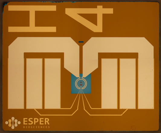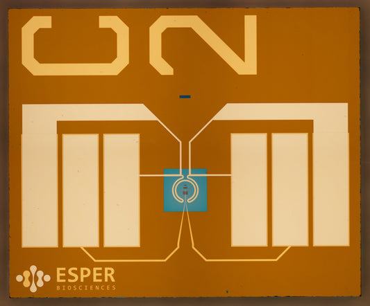
In-situ grids enable electrical transport measurements to be performed simultaneously with TEM imaging.
There are a few grid designs for compatibility with a few different TEM grid holders (see individual product pages).
Features:
- Compatible with a few specialized TEM holders
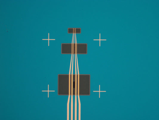
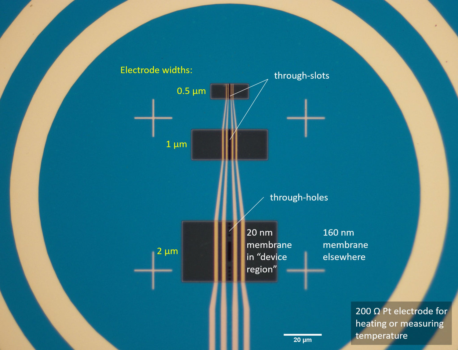
- Three “device regions” having
- Three electrode widths: 0.5, 1, 2 μm to fit a variety of sample sizes
- Electrodes are gold
- Low oxidation
- 25 nm height provides a relatively flat surface (useful for 2D materials)
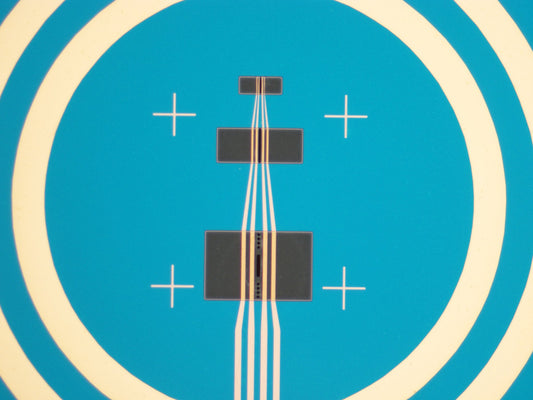
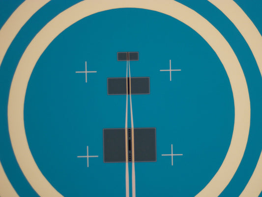
- A thin ~20 nm nitride membrane for low-background imaging
- Holes/slots for background-free imaging
- Slots to allow for imaging at high tilt angle
- Bulk of the membrane is 160 nm for
- Greater durability when depositing samples
- Greater rigidity when imaging
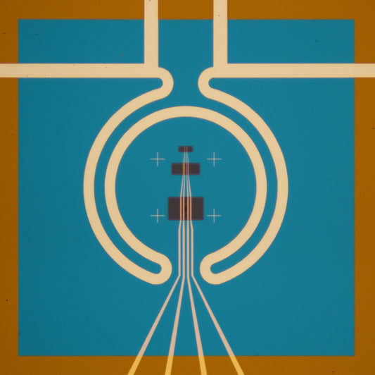
- Pt ring electrodes* allow
- Heating the membrane
- Note: Gold can migrate at high temperatures, so grids may not be suitable for experiments over 400C
- Measuring membrane temperature (via changes in resistance of the 200 Ω ring)
- Heating the membrane
- 4 alignment marks for custom lithography or aligned sample deposition (80 μm spacing)
- Unique device labels readable without a microscope
* All in-situ grids except 3x4-4e
-
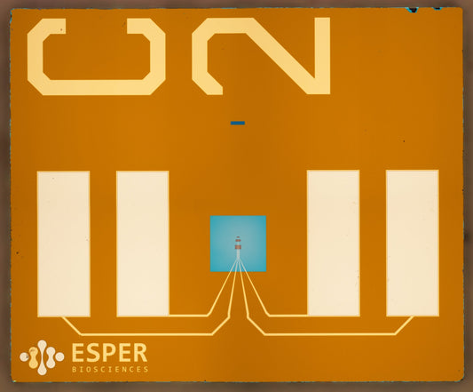
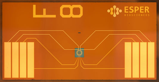
In-situ TEM grid with four electrical and two temperature contacts (5 pack)
Regular price $399.00 USDRegular priceUnit price per -
In-situ TEM grid with two electrical and four temperature contacts (5 pack)
Regular price $399.00 USDRegular priceUnit price per -
In-situ TEM grid with four electrical contacts (5 pack)
Regular price $399.00 USDRegular priceUnit price per -
In-situ TEM grid with four electrical and four temperature contacts (4 pack)
Regular price $399.00 USDRegular priceUnit price per